lab of loto game design⚓
VHDL Cheat⚓
https://memo-vhdl.gitlab-pages.imt-atlantique.fr/
assiocated gitlab repository⚓
A gitlab repository tp-loto-etudiant is available in your gitlab space on https://gitlab-df.imt-atlantique.fr, in the group corresponding to the course followed.
To manipulate it (clone, add, commit, push, pull), please refer to the page Git and Gitlab .
Presentation of the LOTO circuit⚓
Main functions⚓
The circuit to be designed allows a random draw of the LOTO type of 6 different numbers between 1 and 49. The operating principle is as follows: to draw a number, you must press a button, then release it. If the number has not already been drawn, it is displayed and a green diode indicates to the user to move on to the next number, the number drawn being saved in a register of the memory. Otherwise, a red diode lights up to indicate to the operator that he must start the draw again. The numbers in memory scroll in a loop (number designating the read register, tens digit of the number in the register, then units digit) on 7-segment displays. Using a switch, we can block the display of the memory on a register.
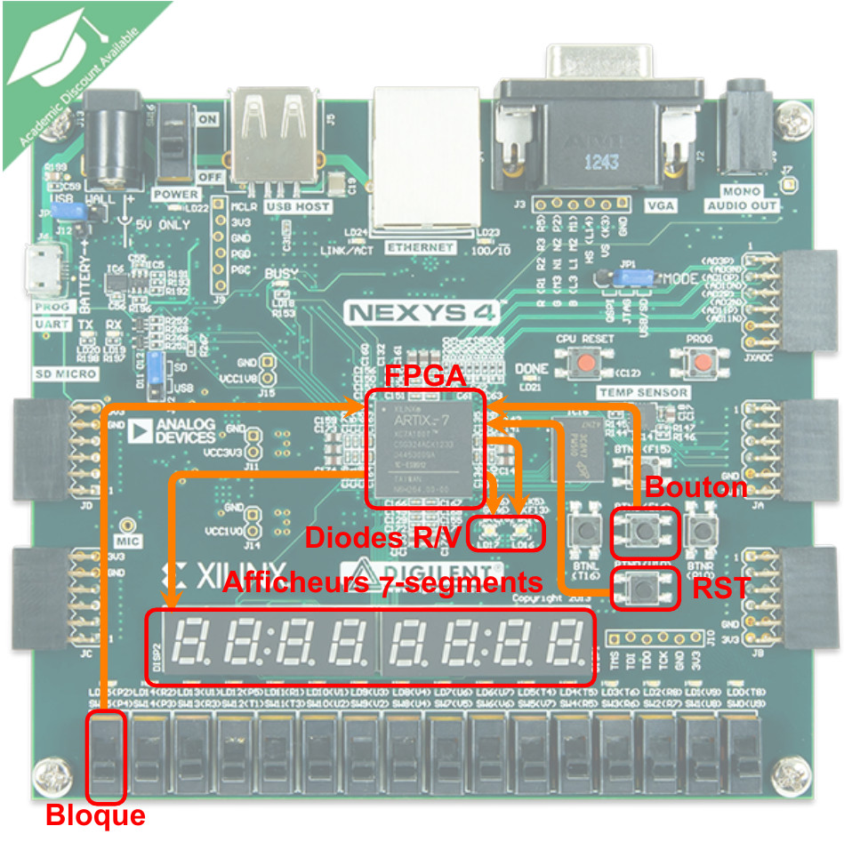
Target hardware⚓
The circuit to be configured is a Xilinx Artix7 (xc7a100tcsg-1) FPGA which is inserted on the Digilent Nexys4 board shown below and including, in addition to the FPGA, the tri-color LEDs, the 7-segment displays, a 100MHz quartz to provide a clock signal, a few components used in particular to control the displays and two buttons: one to reset the circuit, the other to draw the numbers.
Complete Loto circuit⚓
Operating principle⚓
Before drawing the numbers, all the flip-flops of the circuit must be initialized by setting I_rst to 1, then setting it to 0. The displays must then all display 0. Drawing a number is done with a synchronous counter counting from 1 to 49 in a loop. The counter progresses as long as I_button = 1. As soon as I_button = 0, the counter is blocked in its state. The circuit must then:
- memorize the state of the counter in a register if the number has not yet been drawn, and turn on the green LED,
- turn on the red LED if the number has already been drawn.
The six numbers are stored in six output registers feeding the 2 displays (one for the tens and one for the units) of the board. When the sixth valid number is drawn, the red and green LEDs must flash alternately (at a half-second lighting rate) and a new draw can only start by actuating I_rst.
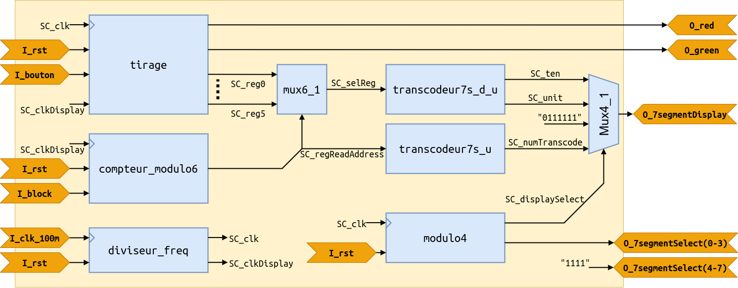
Draw module⚓
Roles of the inputs⚓
| Inputs | Description |
|---|---|
I_clk |
circuit clock provided by a frequency divider circuit based on a signal from a 100 MHz quartz |
I_clk_display |
periodic signal of the order of 1Hz, provided by the aforementioned frequency divider |
I_rst |
reset of the circuit, in particular of the displays |
I_button |
drawing of the number |
Roles of the outputs⚓
| Inputs | Description |
|---|---|
O_l_red |
powers a red LED indicating that the number must be drawn again. |
O_l_red |
powers a green LED indicating that the next number must be drawn. |
O_reg0 to O_reg5 |
numbers in memory that will have to be transmitted to 7-segment displays. |
This module will have to be interfaced with the buttons and displays, which requires some additional modules that are not detailed here, but whose VHDL code you can explore to understand their operation.
Practical work in session⚓
Info
N.B.: The screenshots are made with Vivado 2018.3. Variations may appear with other versions but the logic of the tool is the same. The proposed practices and notions are basic. As you gain in skills, your practices may (should) evolve!
Retrieving the gitlab project on https://gitlab-df.imt-atlantique.fr⚓
A git repository has been created for each student on the school's DFVS gitlab instance https://gitlab-df.imt-atlantique.fr. It contains the VHDL sources necessary for the project, scripts to manage the Vivado project, and a compte-rendu.md file to answer the questions. If you are working in pairs, choose one of the two, and add your colleague as an owner on the project in gitlab.
First, open a terminal: Ctrl+Alt+T
- Create a directory for the UE Électronique and move into it:
Warning
Remember to adapt the path of the command below to your own needs
1 2 | |
- Clone the git repository locally
Warning
Remember to adapt the link of the command below according to the repository on gitlab
1 | |
The git clone command allows you to retrieve the entire git repository with its history of modifications.
You can easily see that this command has allowed you to download with the ls -alsh command in the tp-loto-etudiant-$USER directory.
Project management under Vivado⚓
Warning
Never put spaces, accents or special characters in file or directory names! This is true in general, on Windows as well as on Linux. This is blocking with Vivado in our case here.
Opening Vivado⚓
Under Linux, open a Terminal, move to the working directory of the repository you cloned, with the cd command, and execute the following command:
1 | |
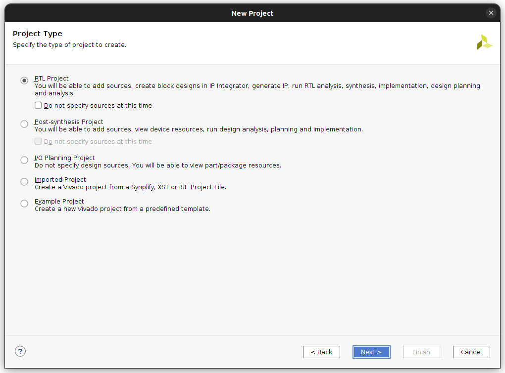
Creating a new project⚓
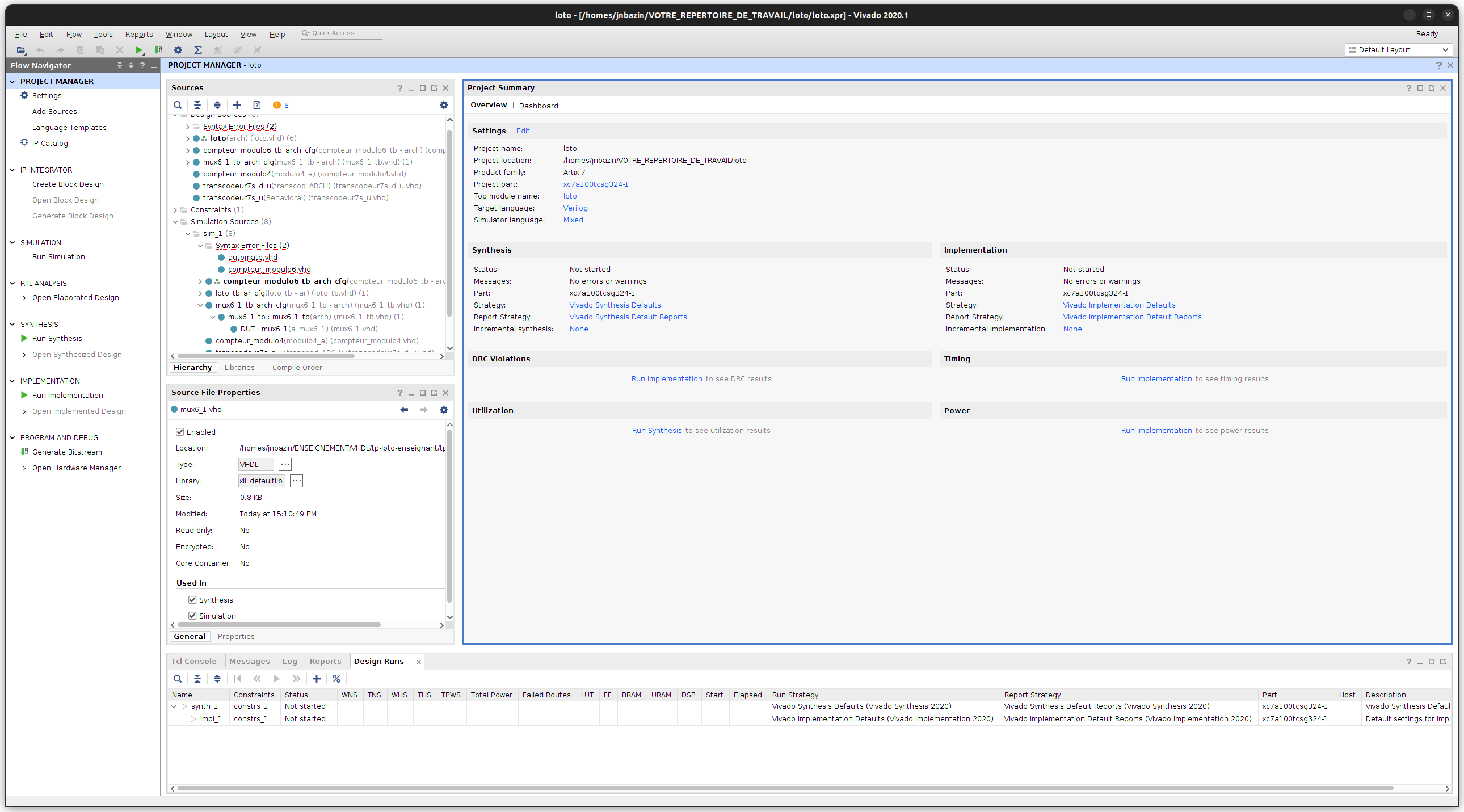
Click on Create New Project to launch the creation assistant (wizard), then click on Next in the window that appears. In the next window:
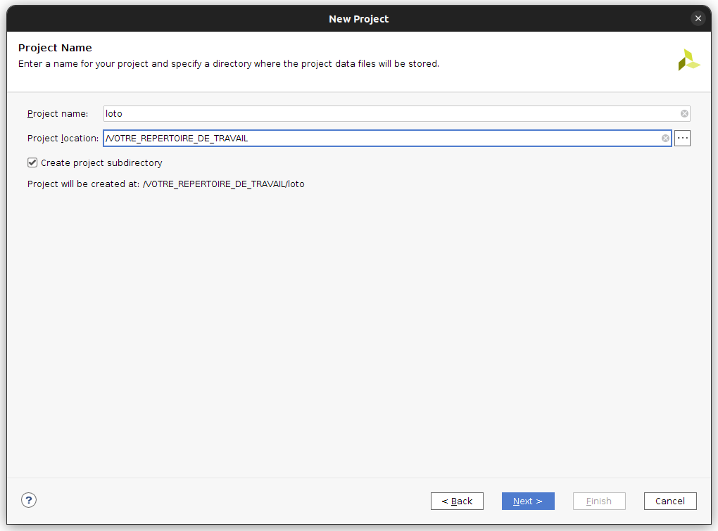
enter the name of your project and your working directory. In the next window, select RTL Project to create a project that will accept VHDL sources.
Adding source files and constraints⚓
Validate again by clicking Next to go to the next window that asks for your source files. Click on Add Files and then select all the VHDL files (with the .vhd extension) from your git repository and then change the mode of the test file loto_tb.vhd to Simulation Only:
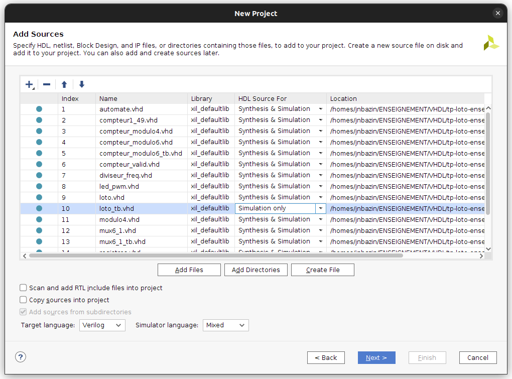
Click Next to validate.
Selection of the target FPGA⚓
Then appears the Add Constraints window. Select the file Nexys4DDR-Master.xdc or Nexys4_Master.xdc depending on the version of the board you have for this TP (a Nexys4 or a Nexys4DDR):
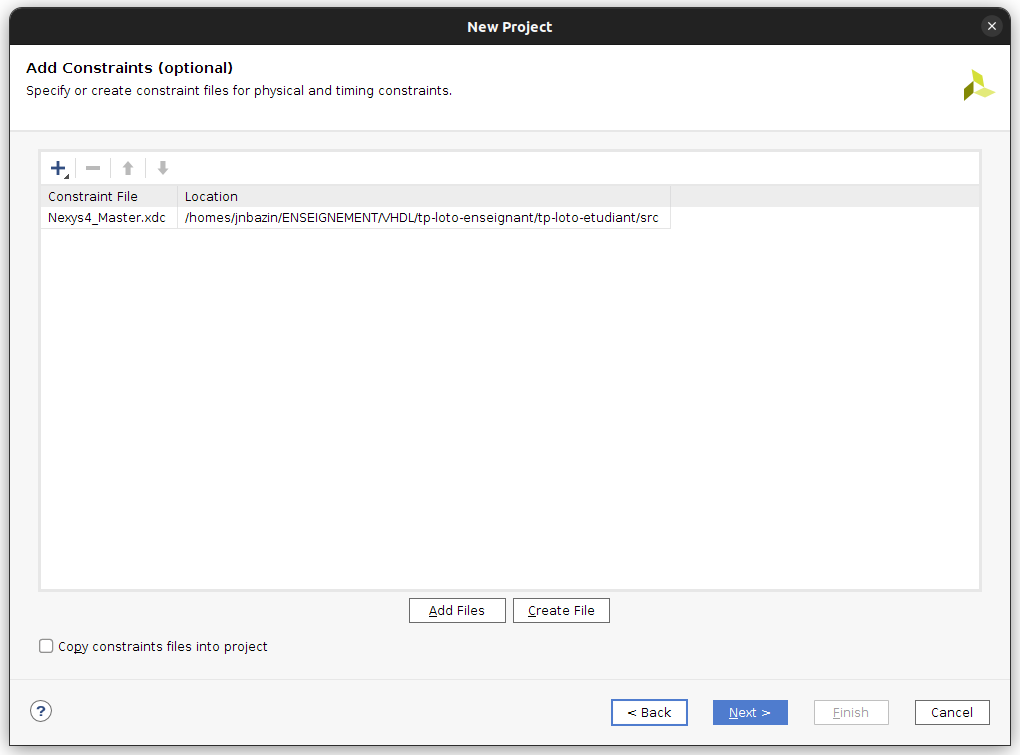
After validation, the window for selecting the FPGA target appears, which you fill in as indicated in the following figure:
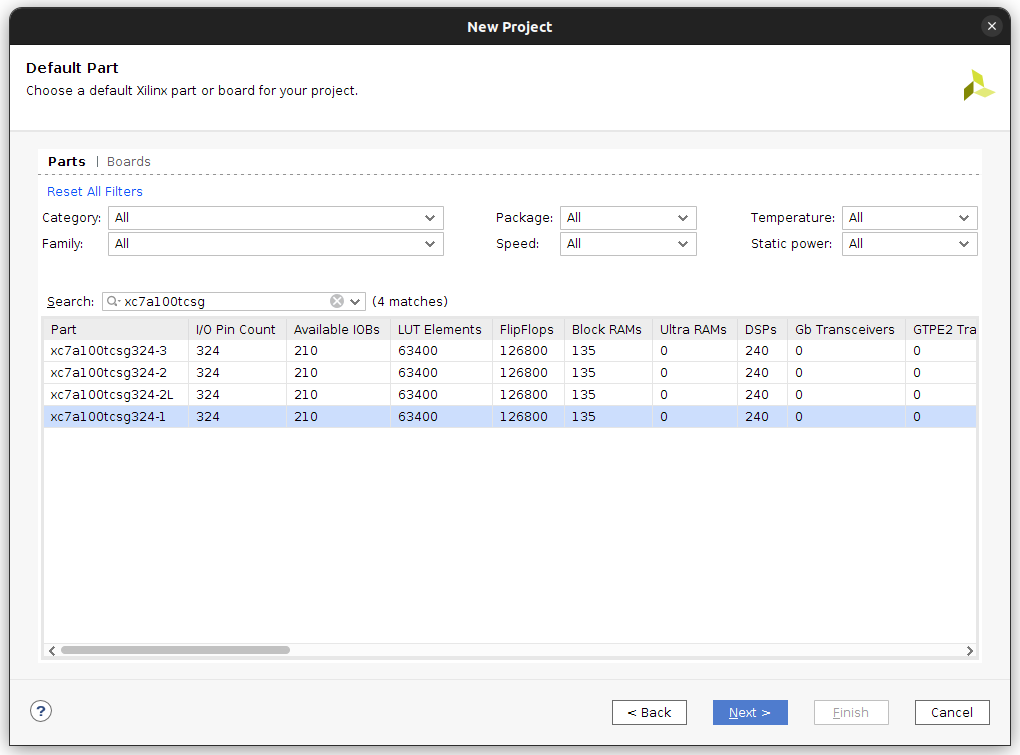
This allows you to choose the FPGA of the Nexys4 (or Nexys4DDR) board. The next window summarizes your project and should be identical to this one:
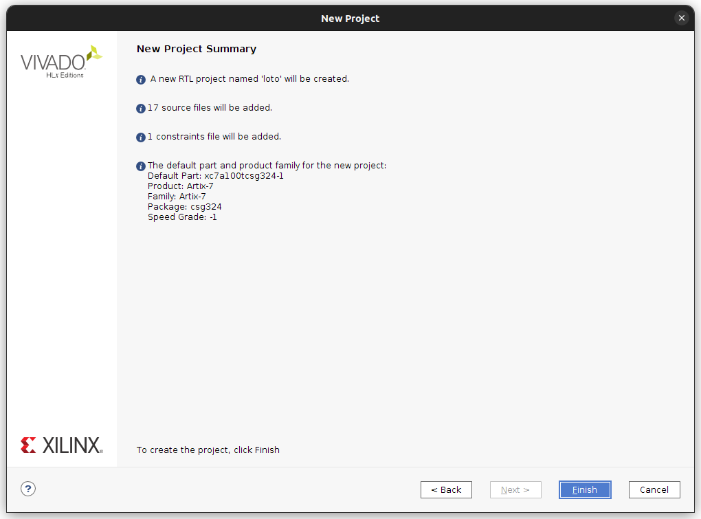
The project is then created and the Vivado project interface is launched:
Partial description of the first combinational module in VHDL⚓
In the PROJECT MANAGER / Sources window, expand the Design Sources / Syntax Error Files item. Open the file mux6_1.vhd, some parts of which have been replaced by _BLANK_. This file allows you to describe a classic combinational function of multiplexing 6 inputs {I_0, I_1, I_2, I_3, I_4, I_5} to an output O_mux6, controlled by a 3-bit signal I_sel. Inspired by the codes presented on https://memo-vhdl.gitlab-pages.imt-atlantique.fr/synthesizable-vhdl/#multiplexer, replace the _BLANK_ sections with appropriate code.
Question Loto 1, (answer to be completed in the docs/compte-rendu.md file)
What signals should be entered in the sensitivity list (if you use an explicit process)?
Question Loto 2, (answer to be completed in the docs/compte-rendu.md file)
What happens if the test at the heart of the process (the succession of "when") is incomplete, i.e. if it does not cover all the input combinations of the module? Is it serious?
VHDL simulation of the first combinational module⚓
To validate your multiplexing module, you simulate it with the XSIM tool of Vivado. For this, a test file is proposed: mux6_1_tb.vhd, also available from the Sources window, Simulation Sources sim_1 /mux6_1_tb_arch_cfg tab. Select this module.
Then, right-click to bring up the context menu and click on Set as Top. This way, this module can be simulated by clicking in the left panel Flow Navigator / Project Manager under the Simulation tab on the Run Simulation command and then on Run Behavioural Simulation.
The window below then appears. Click on Zoom Fit and then adjust the zoom until you can analyze the simulation chronogram and thus check that your VHDL description provides the expected behavior. Do not hesitate to change the display radix of a signal to decimal by clicking on the name of a signal with the right mouse button, then on Radix -> unsigned decimal.
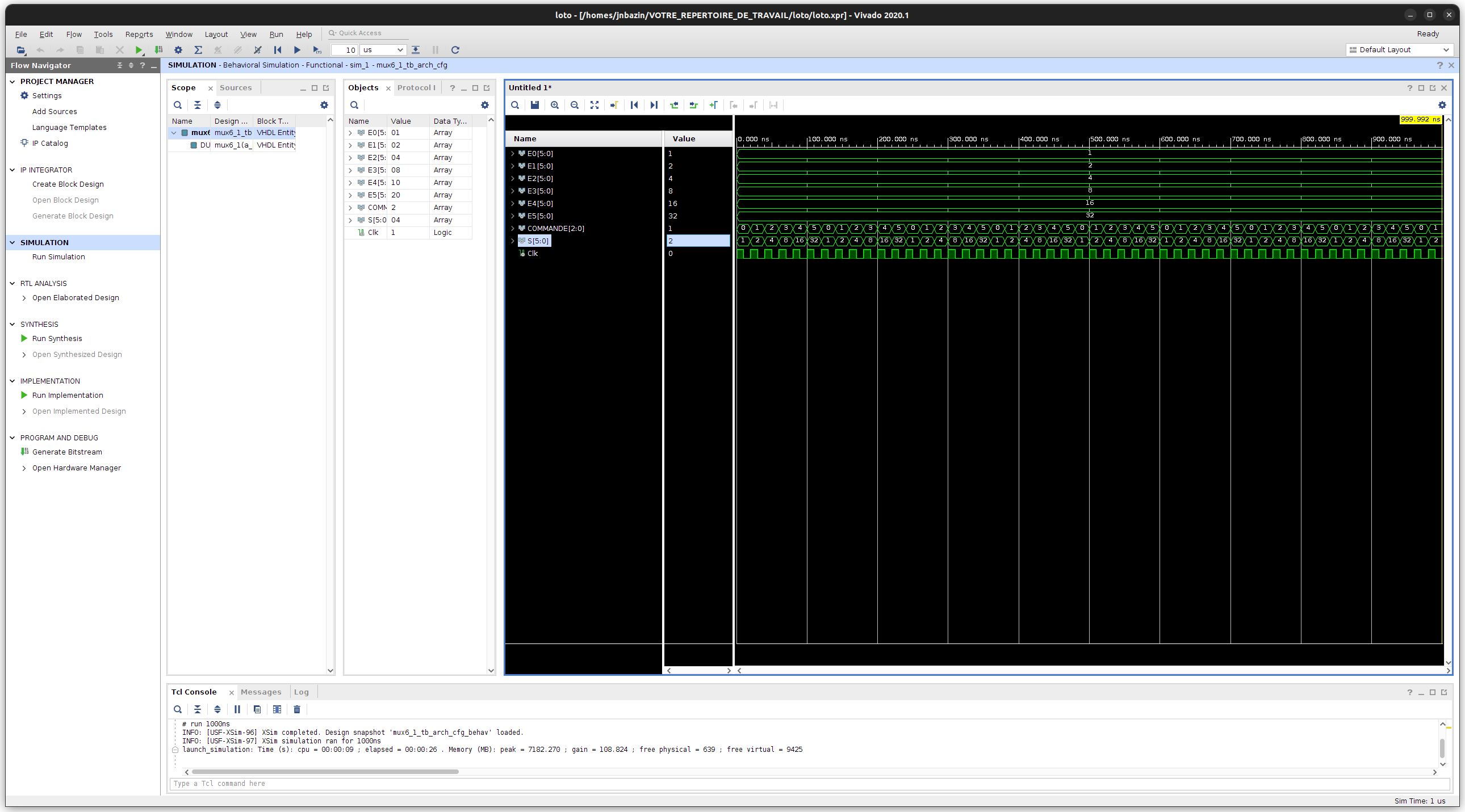
Question Loto 3, (answer to be completed in the docs/compte-rendu.md file)
Is this simulation conclusive? Is it sufficient to validate the module? Justify.
Partial description of the first sequential module in VHDL⚓
Exit the simulation by closing the simulation sub-window. Then, in the PROJECT MANAGER / Sources window, expand the Design Sources / Syntax Error Files tab. Open the file compteur_modulo6.vhd, some parts of which have been replaced by _BLANK_. This file allows you to describe a classic sequential function of counting modulo 6. Inspired by the model provided for a modulo 4 counter provided in the file compteur_modulo4.vhd, replace the _BLANK_ sections with appropriate code.
Question Loto 4, (answer to be completed in the docs/compte-rendu.md file)
What signal(s) should be entered in the sensitivity list of this sequential process? Why?
Question Loto 5, (answer to be completed in the docs/compte-rendu.md file)
What happens if the test is incomplete, i.e. if it does not cover all the input combinations of the module? Is it serious here?
VHDL simulation of the first sequential module⚓
To validate your VHDL description again, you must simulate the module with the proposed test file: compteur_modulo6_tb.vhd.
Question Loto 6, (answer to be completed in the docs/compte-rendu.md file)
Is this test conclusive? Is it sufficient to validate the module? Justify.
Description of a finite state machine⚓
Here is the diagram of the finite state machine that manages the draw:
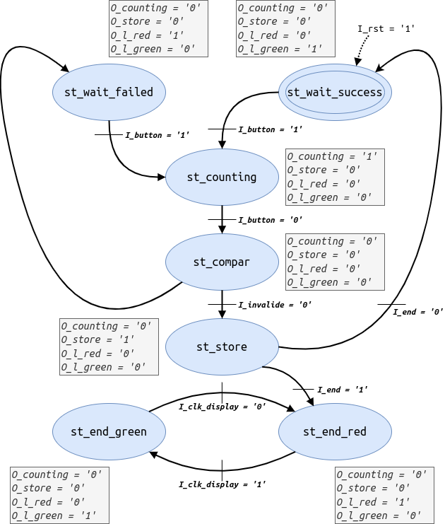
You will describe this automaton in VHDL. To do this, in the PROJECT MANAGER / Sources window, expand the Design Sources / Syntax Error Files tab. Open the file automate.vhd, some parts of which have been replaced by _BLANK_ and correct them.
Question Loto 7, (answer to be completed in the docs/compte-rendu.md file)
How many processes have you described?
Question Loto 8, (answer to be completed in the docs/compte-rendu.md file)
What type(s) are they
Question Loto 9, (answer to be completed in the docs/compte-rendu.md file)
Would it be possible to describe this state machine differently, in terms of the number and type of processes?
Simulation of the complete circuit⚓
To validate the automaton and the other modules by simulation, you must simulate the entire Loto circuit. So set the module loto_tb_ar_cfg to TOP in the Simulation Sources section and simulate the circuit in the same way as for the previous circuits.
Question Loto 10, (answer to be completed in the docs/compte-rendu.md file)
Is this test conclusive? Justify.
Elaboration, synthesis and implementation of the circuit on FPGA⚓
Now that the circuit is validated by simulation, you will move on to the test on the board, if you pass the hardware compilation phases that are elaboration, synthesis, placement and routing successfully! So set the module loto.vhd to TOP in the Design Sources section. Don't forget this step! In the left panel Flow Navigator / Project Manager under the RTL Analysis tab, click on the Open Elaborated Design command and analyze the circuit inferred by the tool.
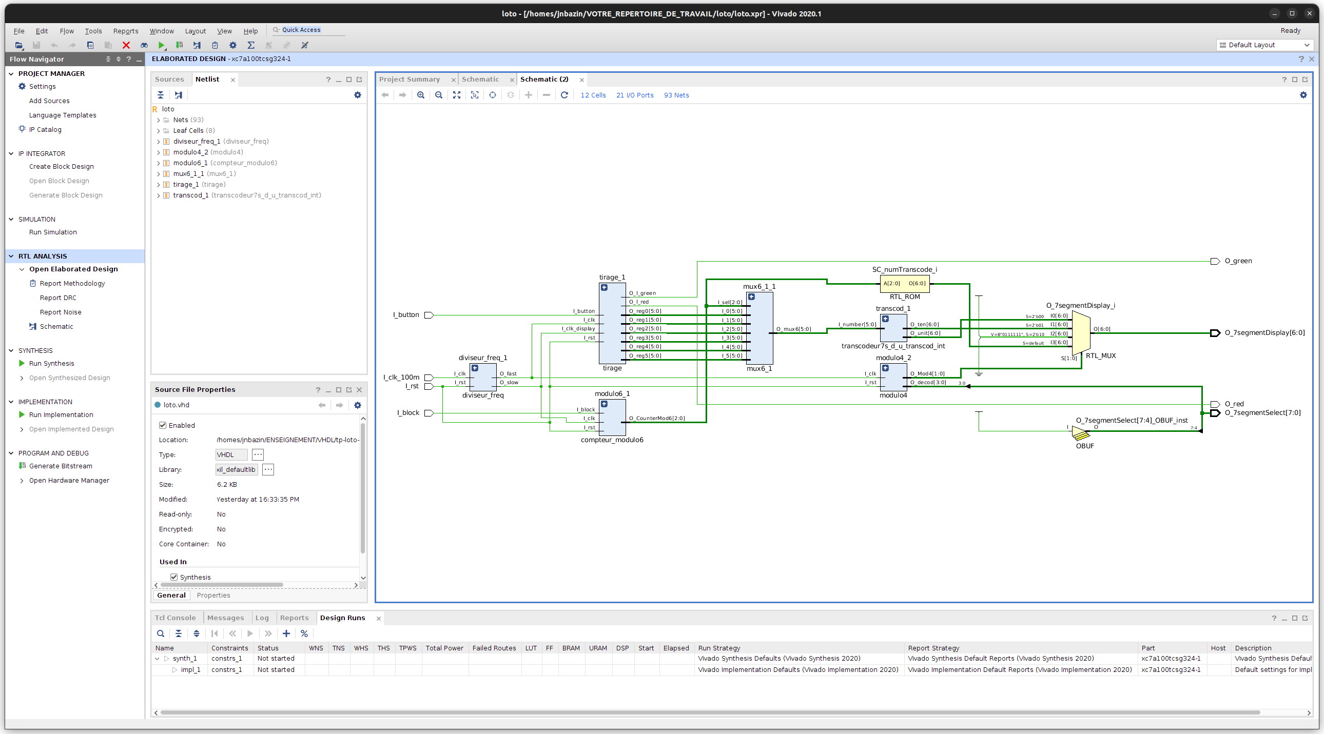
Question Loto 11, (answer to be completed in the docs/compte-rendu.md file)
Is the circuit inferred by the tool consistent with the expected one? If not, how does it differ and is it related to an error in the VHDL description?
Then, still in the left panel Flow Navigator / Project Manager, click on the Run Synthesis command under the Synthesis tab and then accept the default settings. Once the synthesis is finished, Vivado offers you three actions to follow: choose View Reports. In the bottom panel, the Reports tab appears, double-click on the first report in the list: synth_1_synth_report_utilization_0.
Question Loto 12, (answer to be completed in the docs/compte-rendu.md file)
What resources are used on the FPGA? In what quantity/proportion of the available resources? Are LATCHES used? Is this positive or not, why?
Then, you return to the left panel Flow Navigator / Project Manager, click on the Run Implementation command under the Implementation tab and then accept the default settings. When this hardware compilation phase is finished, Vivado offers you three options for the next steps, select Generate Bitstream and then validate the default options. The tool then produces a configuration file for the FPGA that specifies how the FPGA will be used to provide the circuit designed in VHDL and constrained by the file that specifies the inputs/outputs.
Testing the circuit on the FPGA⚓
Once the bitstream generation is finished, you can select the Open Hardware Manager option. Connect a board to a USB port on your computer and make sure that the Power switch is set to ON if no LED lights up before calling a teacher.
In the Hardware manager window, click on Open target in the green banner and then on Auto Connect. Your FPGA then appears in a sub-window Hardware.
Still in the green banner, click on Program device to transfer the bitstream to the FPGA, which will then be configured to perform the Loto circuit you have described in VHDL.
Test it!
Question Loto 13, (answer to be completed in the docs/compte-rendu.md file)
Is the draw random for a human? for a machine? Justify.